Electron Microprobe Lab
An electron microprobe (EMP) or electron probe microanalyzer (EPMA) is a high-magnification microscope that uses electrons, instead of light, to examine a sample. The ARL-SEMQ electron microprobe at Concord University was installed in 2010. It is currently configured with six wavelength-dispersive spectrometers (WDS), Bruker 5030 large-area silicon drift detector (SDD) energy-dispersive spectrometer (EDS), as well as both secondary and backscatter electron imaging. Twin digital video cameras captures images from the visible light optics, either reflected or transmitted light, and can feed a live image to remote users over the internet. Most analytical, X-ray mapping, and electron image capture functions are automated using modern computer hardware.
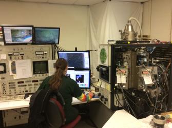
Our ARL SEMQ Electron Microprobe
Most elements from atomic number 6 (C, carbon) through 92 (U, uranium) may be quantitatively analyzed, and elements from atomic number 4 (Be) may be detected. Maximum spatial resolution is about 1 micron (1/1000 of millimeter). For comparison, human hair averages about 50 to 70 microns in diameter. Thus it is possible to both determine what a sample is composed of but also where in the sample specific elements or compounds (e.g. different mineral phases) are located at a microscopic level of detail. Analysis is usually non-destructive, and most natural and synthetic solid materials can be analyzed if properly prepared. For best results, samples should be stable a high vacuum environment, be suitable for polishing to 1 micron or better smoothness, and contain individual particles at least 5 microns in diameter. Typically samples are prepared in circular 25.4 mm (1-inch) diameter mounts or as petrographic thin sections, although other sizes may be accommodated. Non-conductive samples are coated with a thin film of carbon prior to analysis.
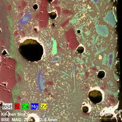
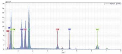
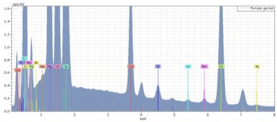
The EDS system is used for rapid qualitative and quantitative analyses as well as X-ray mapping – including spectral imaging and phase discrimination. For most elements, concentrations as low as several hundred ppm are detectable by EDS.
The six WDS spectrometers are used primarily for quantitative analysis. Each is configured with two diffracting crystals (PET and LIF in spectrometer 1, LIF and PET in spectrometer 2, RAP and PET in spectrometer 3, LIF and ADP in spectrometer 4, PET and LIF in spectrometer 5, and PET and TAP in spectrometer 6) and each crystal type allows for the analysis of a different range of elements. Quantitative analysis functions are fully automated using Probe for EPMA software. Computer automation allows large numbers of points, lines, or a combination of both to be analyzed unattended, often overnight. Combined WDS+EDS quantitative analysis is frequently used to provide additional analytical flexibility and improved throughput.
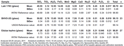
The minimum detection limits and analytical accuracy of a WDS analysis depend primarily on the electron beam conditions (current and accelerating voltage) and the counting times chosen for the analysis. Detection limits of ~100 – 300 ppm are readily attained in many materials. During a typical multi-element analysis of a few minutes duration, 1σ precision of 0.3 – 1.5% relative is normally attained for major elements (i.e. those present at concentrations > 1% by weight). If desired, analytical precision and detection limits may be improved by increasing X-ray acquisition (counting) times, by increasing beam current, and/or by assigning multiple spectrometers to a single element. During analysis of trace Ti in quartz, for example, tuning all six spectrometers to a single element, using high beam current (100nA), and using long analysis times (7 minutes), it it possible to achieve a calculated 3σ (99% confidence) detection limit of 8 ppm.
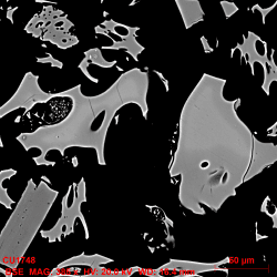
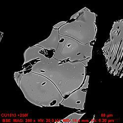
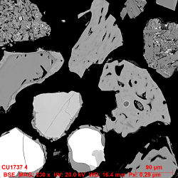
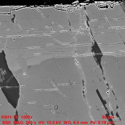
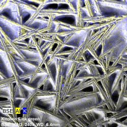
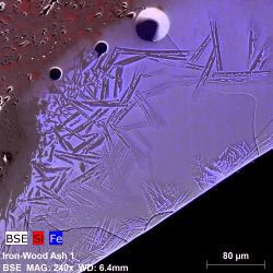
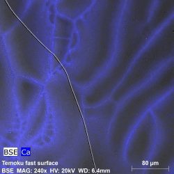
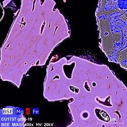
Because the electron microprobe is essentially a specialized scanning electron microscope, it can also be used to collect electron images. Secondary electron images (SEI) are used primarily to reveal surface features and morphology. Backscatter electron images (BSE) can also reveal the size and shape of particles, but are primarily used to provide some spatial information about the sample composition. This is because the intensity of the BSE signal depends on the average atomic number of the sample. Areas richer in heavier elements are brighter in BSE images, and areas consisting primarily of light elements are darker.
The ARL SEMQ design has several advantages. The higher take-off angle at which the spectrometers are positioned (52.5o in the ARL compared to 40o in Cameca and JEOL microprobes) increases light-element sensitivity through reduced absorption of X-rays exiting the sample, reduces matrix corrections for quantitative analysis, and reduces the sensitivity to minor surface topography. The instrument and spectrometers are ruggedly built and therefore durable. The ARL design also supports up to 6 fully-tunable wavelength dispersive (WDS) spectrometers (or up to 12 fixed WDS monochrometers). The more common JEOL and Cameca microprobes have at most 5 WDS spectrometers.
One major application of the microprobe is tephrochronology, the use of volcanic ash and pumice (tephra) as a tool for dating and correlation. Tephrochronology is employed globally with numerous interdisciplinary applications including: environmental and climate change, archaeology, earth surface processes, ecology, animal and plant evolution, earthquake hazards & neotectonics, and volcanic hazards.

